- The study on the Physical Review Letters web site
- The press note on the CNR web site.
Revealing hidden structures in layered materials using light
- /
- News
- /
- Revealing hidden structures in...
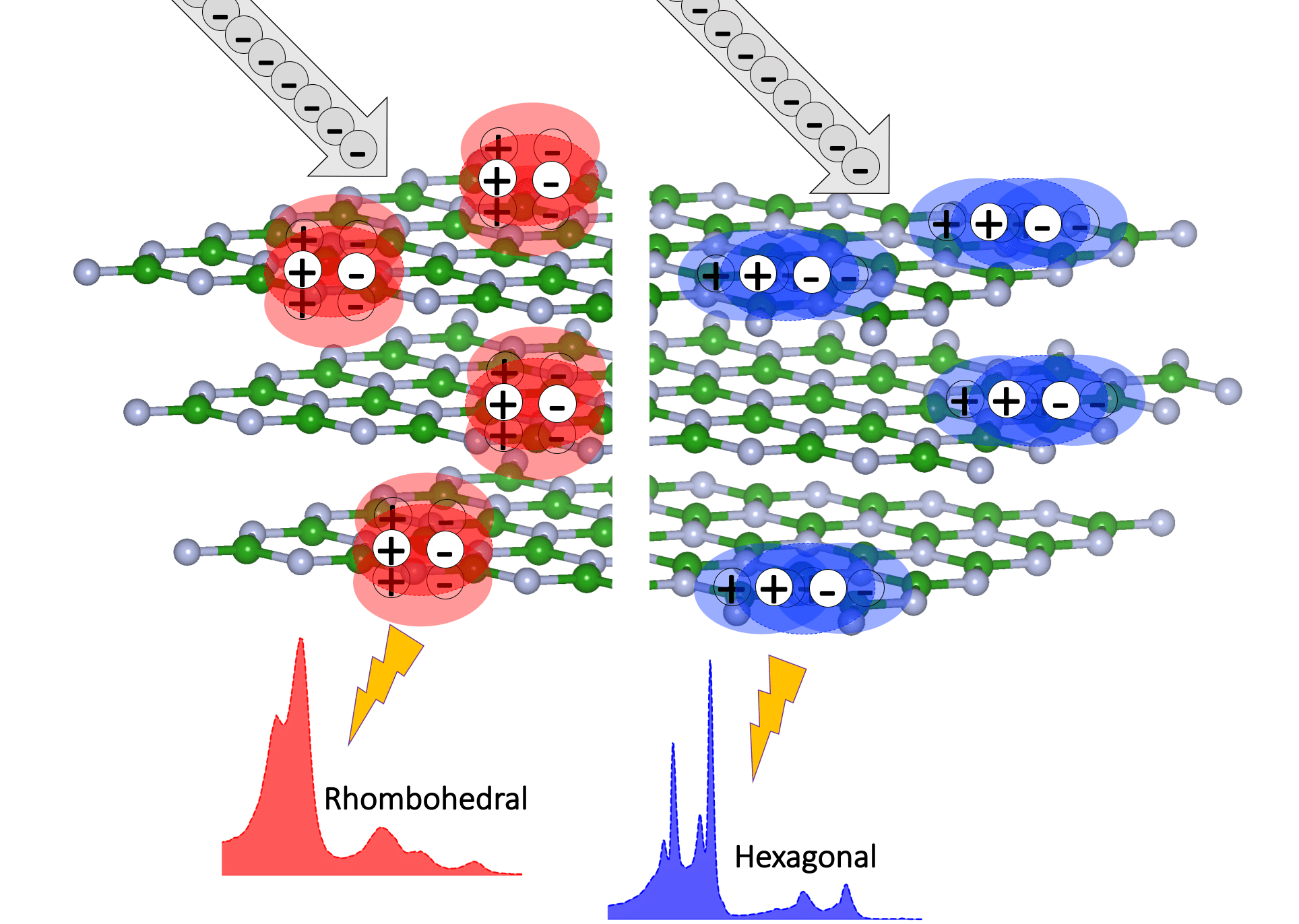
In a combined experimental and theoretical study on ultraviolet-light emission, the CNR Institute of Nanoscience in Modena and the University Paris-Saclay have conducted an important study on a method to discern imperceptible differences in the crystalline structure of layered semiconductor materials: hexagonal boron nitride and rhombohedral boron nitride.
Experimental physicists at the University Paris-Secley conducted measurements with luminescence spectroscopy and analyzed the emitted light spectra displaying characteristic differences between the two similar forms of boron nitride, which differ only in how the atomic layers are superimposed. The Cnr Institute of Nanoscience in Modena researchers, including Fulvio Paleari, Daniele Varsano, Elisa Molinari, and Matteo Zanfrognini, elucidated the observed differences through theoretical simulations on Cineca high-performance supercomputers.
The study was published in Physical Review Letters and bears promising implications for materials design.
“Despite being composed of the same elements, boron and nitrogen, the two forms of the material differ solely in the arrangement of their atomic layers,” explains Daniele Varsano, CNR Nano researcher and co-author of the study. “These structural disparities lead to variations in electronic and structural properties, opening doors to diverse applications—from optoelectronic devices, such as LEDs, to ceramic materials.”
The researchers demonstrated that when an electric current stimulates these materials, the emitted light is a powerful tool to unequivocally differentiate between the two similar forms, effectively isolating the version with desired properties from the other.
“Our simulations show that the distinct symmetries of the crystal lattice in hexagonal and rhombohedral forms influence the characteristics of the emitted light. The dissimilarities in spectra arise from the diverse interactions between vibrating atomic nuclei and the material’s electrons, prompting light emission,” says Fulvio Paleari.
“This study demonstrates that precise measurement of emission spectra is considerably more sensitive to minimal structural differences compared to commonly used experimental techniques. This sensitivity facilitates the easy differentiation of crystalline structures when engineering new materials, ensuring greater control over the final optoelectronic properties,” adds Paleari.
The research was conducted thanks to advanced quantum mechanics software developed within the European Centre of Excellence MaX for theoretical material studies and the National Research Center in HPC, Big Data, and Quantum Computing ICSC.